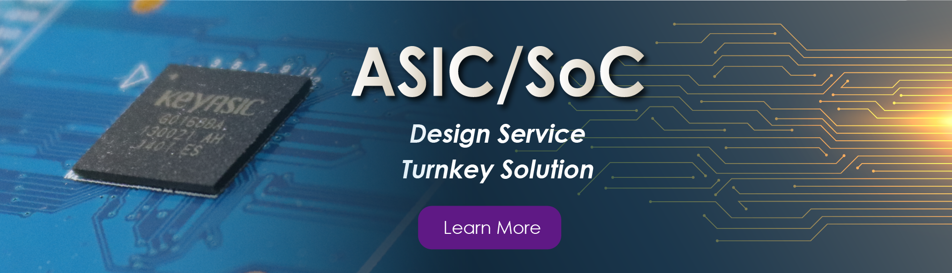
CUSTOM LAYOUT DESIGN ENGINEERS
Job Description
In this position, you will be responsible for physical design implementation. Your scope of work includes but not limited to
- VLSI component layout and translation of schematics into layout geometry
- Participate in module/chip floor planning
- Physical verification includes layout extraction, LVS/DRC verification, signal integrity checks and design for manufacturing checks
- Involve in PDK development and qualification such as physical verification rules (LVS, DRC, OPC, dummification) development and qualification.
- Supports process migration across different foundries.
- Supports tapeout process and silicon debug efforts.
You will work closely with other engineering teams and product marketing teams for end product development. Understanding of library development and characterization is essential, experience in deep sub-micron layout design, integration and interface needs to be continuously strengthened.
Qualifications
The ideal candidate should be knowledgeable in custom layout design with hands-on experience in the design and development of deep sub-micron layout design and integration. He/She must be very familiar and knowledgeable with various custom layout requirements to solve the issues of fringing effect of leakage, noise, and power consumption. Exceptional knowledge from full custom layout development, characterization and timing model generation is required. Working experience in development of domain-specific application chip is a plus. The ability to work with and develop relationships with multiple function groups and execute in a fast paced environment is essential.
Required Education:
Previous experience in full custom layout development is required. Advanced degree in an engineering discipline is preferred.
|